The Materials Scientist's Guide to Publication-Ready Figures: XRD, SEM, TEM, and Spectroscopy Plots in 2025

Materials characterization generates some of the most visually demanding figures in all of science. An XRD pattern with overlapping peaks, a TEM micrograph with an inset diffraction pattern, or a set of stress-strain curves for five alloy compositions - these are not simple bar charts. They carry dense quantitative information and must survive peer review at journals like Acta Materialia, ACS Nano, and Advanced Materials.
This guide covers the specific figure conventions that materials scientists encounter daily. Every section includes complete, runnable Python code you can adapt to your own datasets, or you can skip the manual coding entirely and generate publication-ready figures with Plotivy.
What This Guide Covers
0.Live Lab: XRD Stacked Patterns
1.XRD Pattern Best Practices
2.SEM and TEM Image Figures
3.Spectroscopy Overlays (Raman, FTIR, UV-Vis)
4.Live Lab: Stress-Strain Curves
5.Common Materials Science Figure Mistakes
6.Quick Reference Checklist
Live Lab: XRD Stacked Patterns
Edit the code below to change alloy compositions, add Miller index labels, or adjust peak positions. Click Run to regenerate the figure instantly.
1. XRD Pattern Best Practices
X-ray diffraction patterns are the bread and butter of materials characterization. Whether you are comparing phase compositions across synthesis conditions or confirming the absence of impurity peaks, the way you present XRD data matters. Reviewers expect specific conventions that differ from generic line plots.
Offset Stacking for Multiple Samples
- Normalize each pattern to its own maximum before stacking so that minor-phase peaks remain visible.
- Use a consistent offset increment - typically 1.0 to 1.2 times the normalized maximum.
- Label each pattern directly on the plot, not in a separate legend box.
- Annotate key peaks with Miller indices using matplotlib's
annotate()function. - If including a JCPDS/ICDD reference pattern, place it at the bottom with vertical bars.
2. SEM and TEM Image Figures
Electron microscopy images require a different treatment than data plots. The core challenge is presenting image data at publication resolution while preserving details that reviewers need to evaluate - grain boundaries, nanoparticle distributions, lattice fringes, or diffraction patterns.
SEM Image Checklist
- -Export as TIFF at instrument resolution (no JPEG compression)
- -Include a calibrated scale bar (not the instrument info bar)
- -Accelerating voltage and working distance in the caption
- -Use consistent magnification across comparison panels
- -Adjust contrast/brightness uniformly across all images in a figure
TEM Image Checklist
- -Report lattice spacings in the caption for HRTEM images
- -Include SAED patterns as insets with labeled diffraction spots
- -FFT insets should include a scale bar in reciprocal space
- -Multi-panel: (a) bright-field, (b) SAED, (c) HRTEM with FFT inset
- -EDS maps: use consistent color mapping and include the element label
Try it
Try it now: review your figure before submission
Upload your current plot and get an AI critique with concrete fixes for clarity, typography, color, and journal readiness.
Open AI Figure Reviewer →Newsletter
Get a weekly Python plotting tip
One concise tip each week for cleaner, faster scientific figures. Built for researchers who publish.
Pro tip: Use matplotlib's plt.subplots(1, 3, figsize=(12, 4)) for SEM/TEM multi-panel figures. Set ax.set_aspect('equal') to prevent distortion and remove axis ticks with ax.axis('off').
3. Spectroscopy Overlays (Raman, FTIR, UV-Vis)
Spectroscopy data shares many conventions with XRD patterns but has its own quirks. FTIR spectra traditionally plot transmittance with an inverted y-axis. Raman spectra use relative wavenumber shifts. UV-Vis data can show absorbance, transmittance, or reflectance depending on the application.
Spectroscopy Figure Conventions
Raman
- X-axis: Raman Shift (cm-1)
- Y-axis: Intensity (a.u.)
- Annotate D, G, 2D bands
- Include excitation wavelength
FTIR
- X-axis: Wavenumber (cm-1), reversed
- Y-axis: Transmittance (%)
- Label functional group peaks
- Use offset stacking for samples
UV-Vis
- X-axis: Wavelength (nm)
- Y-axis: Absorbance (a.u.)
- Mark absorption edge / band gap
- Include Tauc plot inset if needed
4. Live Lab: Stress-Strain Curves
Edit the alloy parameters below to see how yield strength, UTS, and elongation change the curve shape. The code automatically marks the 0.2% offset yield point and annotates UTS.
Try with your own data
Load a built-in materials science dataset and generate figures automatically.
5. Common Materials Science Figure Mistakes
Low-Resolution Micrographs
Exporting SEM/TEM images as JPEG introduces compression artifacts. Always export as TIFF or PNG at the instrument's native resolution.
Misaligned Stacked Patterns
XRD or spectroscopy patterns with unequal offsets make peak comparison impossible. Use a consistent offset increment.
Missing Scale Bars
Never rely on axis-based sizing for microscopy. A calibrated scale bar burned into the image is mandatory for all SEM/TEM panels.
Overcrowded Legends
Five overlapping curves with a 10-entry legend is unreadable. Label curves directly on the plot or use a clean, separated legend.
Unlabeled Peaks
XRD patterns without Miller indices or phase labels force reviewers to guess. Annotate every significant peak.
Wrong Stress-Strain Convention
Mixing true stress with engineering strain, or reporting strain as a fraction instead of percent without labeling. Be explicit in axis labels.
6. Quick Reference Checklist
| Figure Type | Resolution | Format | Key Requirement |
|---|---|---|---|
| XRD Patterns | 300 DPI | PDF/EPS | Miller indices, reference sticks |
| SEM Images | Native px | TIFF | Scale bar, kV, WD in caption |
| TEM / HRTEM | Native px | TIFF | Lattice spacings, SAED inset |
| Raman/FTIR | 300 DPI | PDF/EPS | Functional group labels |
| Stress-Strain | 300 DPI | PDF/EPS | 0.2% yield marker, UTS label |
Chart gallery
Materials Science Chart Templates
Browse ready-made chart types commonly used in materials research.
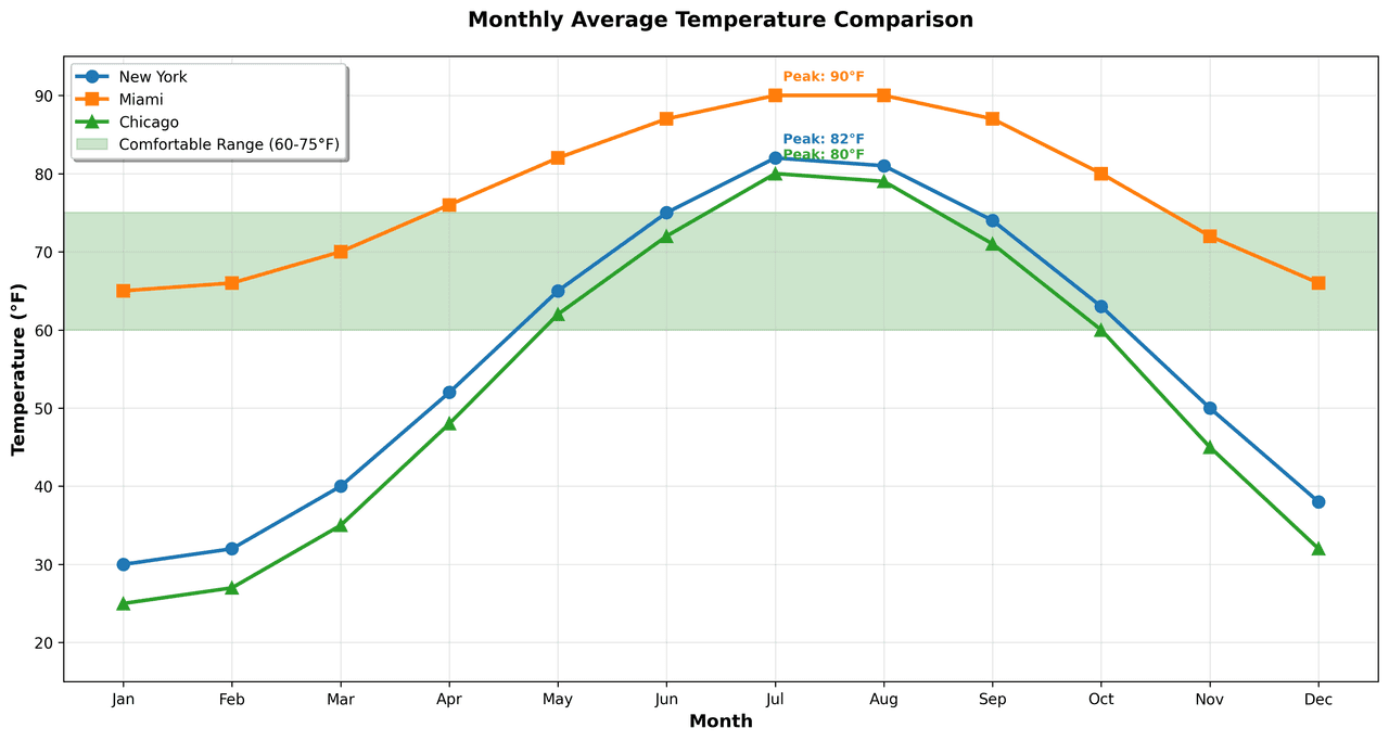
Line Graph
Displays data points connected by straight line segments to show trends over time.
Sample code / prompt
import matplotlib.pyplot as plt
import numpy as np

# Generate temperature data for 3 major US cities over 12 months
months = ['Jan', 'Feb', 'Mar', 'Apr', 'May', 'Jun', 'Jul', 'Aug', 'Sep', 'Oct', 'Nov', 'Dec']
nyc = [30, 32, 40, 52, 65, 75, 82, 81, 74, 63, 50, 38]
miami = [65, 66, 70, 76, 82, 87, 90, 90, 87, 80, 72, 66]
chicago = [25, 27, 35, 48, 62, 72, 80, 79, 71, 60, 45, 32]

# Create figure with enhanced styling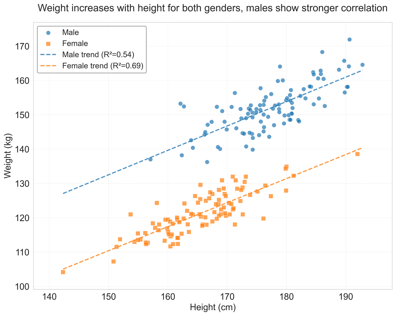
Scatterplot
Displays values for two variables as points on a Cartesian coordinate system.
Sample code / prompt
import matplotlib.pyplot as plt
import numpy as np
from scipy import stats
import pandas as pd

# Generate sample data
np.random.seed(42)
n_samples = 200
height = np.random.normal(170, 8, n_samples)
weight = height * 0.6 + np.random.normal(0, 8, n_samples) - 50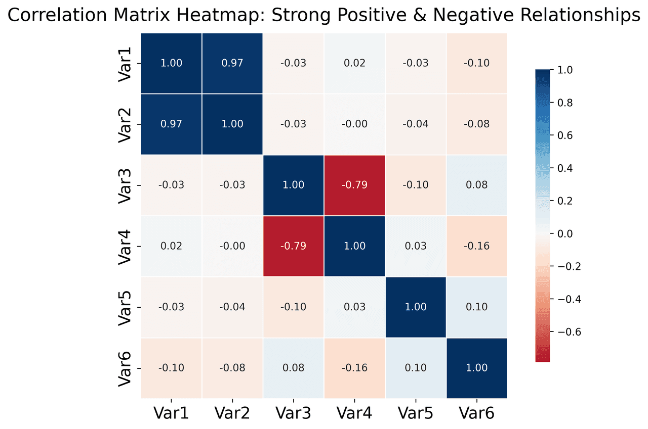
Heatmap
Represents data values as colors in a two-dimensional matrix format.
Sample code / prompt
import matplotlib.pyplot as plt
import seaborn as sns
import pandas as pd
import numpy as np

# Create correlation matrix for financial metrics
metrics = ['Revenue', 'Profit', 'Expenses', 'ROI', 'Customers', 'AOV', 'Marketing', 'Employees']
correlation_data = np.array([
    [1.00, 0.85, -0.45, 0.72, 0.88, 0.65, 0.72, 0.55],
    [0.85, 1.00, -0.78, 0.92, 0.75, 0.58, 0.63, 0.48],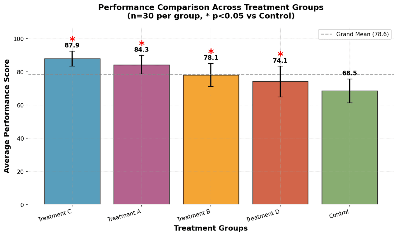
Bar Chart
Compares categorical data using rectangular bars with heights proportional to values.
Sample code / prompt
import numpy as np
import pandas as pd
import matplotlib.pyplot as plt
import seaborn as sns
from scipy import stats

# Generate performance scores for 5 treatment groups
np.random.seed(42)
groups = ['Control', 'Treatment A', 'Treatment B', 'Treatment C', 'Treatment D']
n_samples = 30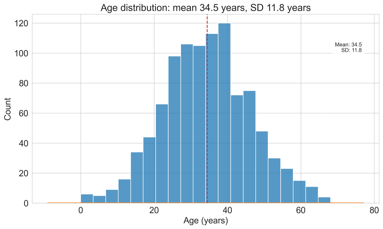
Histogram
Displays the distribution of numerical data by grouping values into bins.
Sample code / prompt
import matplotlib.pyplot as plt
import numpy as np
from scipy.stats import gaussian_kde, skewnorm

# Generate age data with slight right skew
np.random.seed(42)
ages = skewnorm.rvs(a=2, loc=42, scale=15, size=500)
ages = np.clip(ages, 18, 80)  # Clip to realistic range

fig, ax = plt.subplots(figsize=(12, 7))Generate Materials Science Figures in Seconds
Upload your XRD, spectroscopy, or mechanical testing data and let AI produce publication-ready figures - no manual matplotlib coding required.
Start CreatingTechnique guides scientists read next
scipy.signal.find_peaks guide
Tune prominence and width parameters for robust peak extraction.
Savitzky-Golay smoothing
Reduce noise while preserving peak shape and position.
PCA visualization workflow
Move from high-dimensional measurements to interpretable components.
ANOVA with post-hoc brackets
Add statistically correct pairwise significance annotations.
Found this helpful? Share it with your network.
Experimental Physicist & Photonics Researcher
Hands-on experience in silicon photonics, semiconductor fabrication (DRIE/ICP-RIE), optical simulation, and data-driven analysis. Built Plotivy to help researchers focus on discoveries instead of data struggles.
More about the authorVisualize your own data
Apply the techniques from this article to your own datasets. Upload CSV, Excel, or paste data directly.